The study, simulation and development of storage elements and devices with destructive and non-destructive readout on nanoscale ferroelectric films
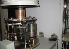
The new technology of deposition of nanoscale (20-50 nm) ferroelectric films (NFF) for the non-volatile memory elements (ME), including the method of RF magnetron sputtering with closed drift of high-energy secondary electrons. Processed using the method and means of RF sputtering plazma monolithic ceramic targets based compounds zirconium, titanium, lead in the direction of reducing the thickness of the film, the technology of ultrasound treatment NFF, which provides an increase in the polarization reorientation and reduction of stress reversal. A new computer model of ME on the NFF, which implements a step-by-step integration of transients as a superposition of a large number of switching processes of the ferroelectric dipoles and calculates the total result of the current, voltage and charge polarization under the influence of ME pulse recording, reading and interference. The values of the ME parameters necessary for the design of memory devices and integrated circuits in SPICE. Made to scale-model ME on NFF with improved options and performance: voltage - 3V, cycle read / write - 40/50 ns, the number of write / read - 1012/1015.
A technology and models of memory elements tested at Research Institute for Microenterprises and the Institute for Nuclear Research of NASU towards design and engineering standards to the world, aimed at solving the problem of creating a universal electronic memory of computer systems, as well as samples of memory chips for general and special-purpose the domestic industry.

| Вложение | Размер |
|---|---|
| 330.5 КБ |


