The creation of the design and manufacture of integrated circuits ferroelectric memory
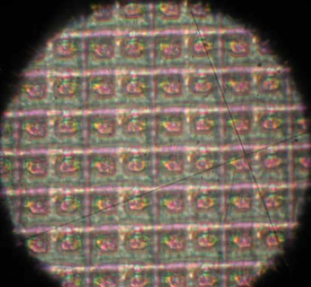
The new research technology to deposition of submicron (20-100 nm) ferroelectric thin films (FTF) for acoustic-volatile ferroelectric storage elements. Improved equipment for deposition and etching of FTF on silicon substrates with CMOS structures and construction of cathode with a circular target and disk fragments, which ensures uniform thickness and composition of FTF during their deposition method ion-plazmа sputtering in magnetron-type reactor with closed drift of electrons. An ultrasonic treatment of FTF at the stage of crystallization, which leads to a reduction of the switch, increasing switching and charge storage volume resistance elements. The methods for applying electrodes to the FTF with a substratum of conducting oxides. The mathematical and computer models of storage elements for use in CAD of IC. Processed technological route and made the layout of the experimental design of integrated circuits "universal" memory density and speed 1 Mbit/sm2 a read/writ 30-40 ns, which allows to serve as the operational and long-term volatile storage of electronic systems.
Results patent is competitive in terms of technology and implementation of structural devices.
Results of the work in the educational process of teaching "Computer Design Basics" and "Computer Architecture", introduced new sections, "Ferroelectric storage device" and "Types and
nomenclature of integrated memory chips.
The technology and structure of memory cells tested in the business enterprise Microdevices
Research Institute, Institute for Nuclear Research and the Institute of Semiconductor Physics NASU towards a design by world standards for semiconductor memory, aimed at solving the current problem of creating a single e-memory computer systems, and the creation of designs memory chips for the
domestic industry.


